Image:Diode.jpg
From Wikimization
(Difference between revisions)

Size of this preview: 692 × 599 pixels
Full resolution (3510 × 3040 pixel, file size: 784 KB, MIME type: image/jpeg)
| Line 5: | Line 5: | ||
3''')''' static semiconductor & contact resistivity R_d a.k.a parasitic resistivity. | 3''')''' static semiconductor & contact resistivity R_d a.k.a parasitic resistivity. | ||
'''('''b''')''' Figure 211b unbalancing and consolidation to help explain high median impedance of diffusion capacitor. | '''('''b''')''' Figure 211b unbalancing and consolidation to help explain high median impedance of diffusion capacitor. | ||
| - | [[https://www.convexoptimization.com/TOOLS/Sedra.pdf PSPICE DEVICE MODELS & SIMULATION]] | + | [[https://www.convexoptimization.com/TOOLS/Sedra.pdf PSPICE DEVICE MODELS & SIMULATION, App.B.1.2]] |
Current revision
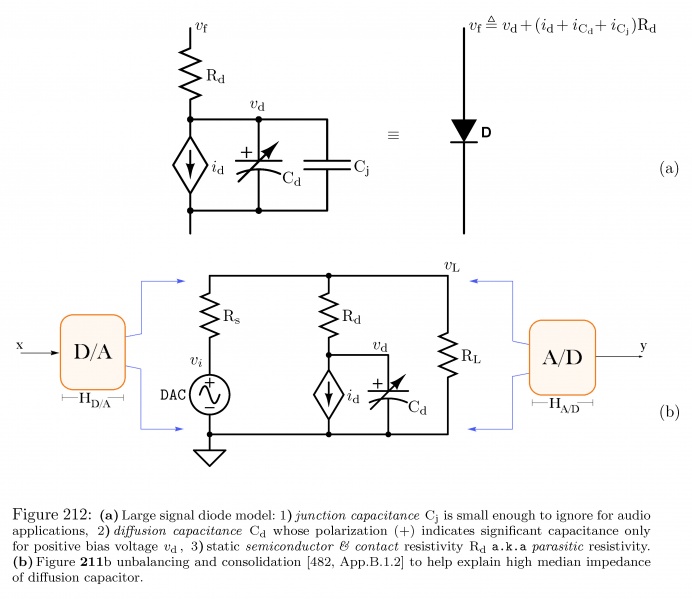
Diode test circuit model from Convex Optimization & Euclidean Distance Geometry, Chapter 8.1. (a) Large signal diode model: 1) junction capacitance C_j is small enough to ignore for audio applications, 2) diffusion capacitance C_d whose polarization (+) indicates significant capacitance only for positive bias voltage v_d , 3) static semiconductor & contact resistivity R_d a.k.a parasitic resistivity. (b) Figure 211b unbalancing and consolidation to help explain high median impedance of diffusion capacitor. [PSPICE DEVICE MODELS & SIMULATION, App.B.1.2]
File history
Click on a date/time to view the file as it appeared at that time.
| Date/Time | User | Dimensions | File size | Comment | |
|---|---|---|---|---|---|
| (current) | 15:39, 16 January 2025 | Ranjelin (Talk | contribs) | 3510×3040 | 784 KB | Diode test circuit model. |
- Edit this file using an external application
See the setup instructions for more information.
Links
The following pages link to this file: